Detectors
Micron Semiconductor
The main part of our own particle detection kit consists of silicon detectors from Micron Semiconductor Ltd.
On Micron’s website one can find their latest product catalogue giving specifications of their various detector types.
On this page, we have backed up their catalogue from 2018, 20??, …
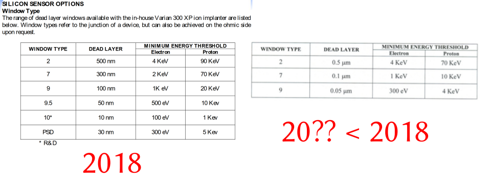
Note: Over time, the specifications given in Micron’s product catalogues have been changing. For example, the dead layer thicknesses of various window types are given in one form in the 2018 catalogue and in another form in an older catalogue (exact year unknown), as shown in the following image

A few additional notes:
- Micron tends to refer only to the doping of the detectors when they speak of deadlayers; i.e. the metal contacts are not deadlayers in Micron’s own terms.
- The thickness of aluminium coverage reported by Micron has changed over time from 2000 Å through 3000 Å up to 2018’s reported 0.5 µm.
- Tolerances on the various measures of Micron’s detectors are an entirely different, and unknown, matter – expect at least 10% variation on all reported thicknesses, including the thicknesses of the active regions of the detectors.
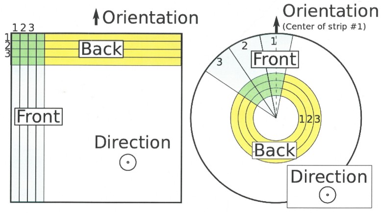
The way we index the strips of Micron’s W1 and S3 detectors in our analysis software AUSAlib is illustrated in the following image.

In both cases, one is looking at the front side of the detectors, and when the orientation is pointing upwards, the connector of the detector is on the bottom.
Below you will find technical drawings and similar of the detector types from Micron which we utilise in the group and a tabulation of our various detectors and their characteristics.
W1 (MSX25 compatible)
On the front-side/p-side of our 9G/2M W1 detectors there is an aluminium grid of thickness 200 nm (electrical contacts) covering 3-4% of the detector surface, followed by a dead layer of 100 nm silicon. Underneath these two effective dead layers is the active detector volume of silicon. Continuing through the material layers of the detector, there is then a dead layer of 500 nm silicon, followed by aluminium strips of thickness 200 nm covering ~98% of the detector surface.
Detailed drawing of W1 profile (with dimensions). According to Neil from Micron Semiconductors, the height of the oxide is \(\approx 1\) \(\mu\)m and the depth of the deep doping is \(\approx 500\) nm. The drawing is a modification of the drawing in O. Tengblad et al, “Novel thin window design for a large-area silicon strip detector”, Nucl. Instrum. Methods. Phys. Res. A 525 (2004) 458-464 – be careful not to treat any one source as the authoritative source on these things (cf. the evolution of the Micron product catalogue over time). Refer also to the more recent paper S. Viñals et al, “Calibration and response function of a compact silicon-detector set-up for charged-particle spectroscopy using GEANT4”, Eur. Phys. J. A (2021) 57:49.
NIM paper from 2013 discussing interstrip effects in W1 detectors: Torresi et al.
See also pages 23-24 in Sheila Lærkegaard Johansen’s Master’s thesis, “A Study of the β- Response of Silicon Detectors and the Effects of Backscattering in a Complex Setup using GEANT4”, AU 2021 and this document provided by Olof which refers to an older Micron catalogue with different specifications.
In the following table, a Right-angled connector type looks as in this drawing, and a Straight connector type looks as in this drawing.
| ID | WAFER NO. |
YEAR PURCHASED |
THICKNESS (um) | TYPE | DEPLETION VOLTAGE (V) |
CONNECTOR TYPE |
PHYSICAL LOCATION |
SPEC SHEET |
COMMENTS |
|---|---|---|---|---|---|---|---|---|---|
| AUW1_40_00 | 3203-11 | 2019 | 40 | 9G/2M | 12 | Right-angled | Aarhus | link | |
| AUW1_50_00 | 3189-3 | 2015 | 55 | 9G/2M | 9 | Right-angled | Aarhus | link | |
| AUW1_50_01 | 3188-5 | 2015 | 55 | 9G/2M | 20 | Right-angled | Aarhus | link | |
| AUW1_60_00 / MD0007 |
? | 2008? | ~60 | ?G/2M | ? | Straight | Aarhus | - | From I. E. M. Madrid; used in IS999 |
| - | 3187-4 | 2015 | 60 | 9G/2M | 20 | ? | link | ||
| - | 3187-5 | 2015 | 60 | 9G/2M | 25 | ? | link | ||
| AUW1_60_03 | 2410-14 | 2020 | 61 | 9G/2M | 8.5 | Straight | Aarhus | link | |
| AUW1_60_02 | 2887-4 | 2011 | 65 | 9G/2M | 10 | Right-angled | Aarhus | link | |
| AUW1_60_01 | 2881-1 | 2011 | 67 | 9G/2M | 10 | Right-angled | Aarhus | link | |
| AUW1_65_00 | 2846-5 | 2017 | 68 | 2M/2M | 10 | ? | link | ||
| AUW1_65_01 | 3187-1 | 2017 | 70 | 2M/2M | 24 | ? | link | ||
| - | 3102-14 | 2015 | 295 | 9G/2M | 50 | ? | link | ||
| AUW1_300_00 | 3102-13 | 2015 | 296 | 9G/2M | 45 | Right-angled | ? | link | |
| AUW1_500_00 | 2495-18 | 2012 | 524 | 9G/2M | 40 | Right-angled | Aarhus | link | |
| AUW1_1000_00 | 2541-7 | 2019 | 1002 | 9G/2M | 85 | Right-angled | Aarhus | link | |
| AUW1_1000_01 | 2947-4 | 2019 | 1043 | 9G/2M | 146 | Right-angled | Aarhus | link | B-Grade |
S3
Technical drawing 2 (special connector).
S3 specs – consult also the latest Micron product catalogue.
Neil could not provide us with a detailed drawing of the S3 profile. However, he gave this description: The S3 detector is a little more complicated in terms of the layer structure on the front when compared to the W1 as uses a double metal process. However, the junction implant is only a type 2 with a 0.5um depth. On top of silicon junction is metal 1 at 0.6 um, then 3.5 um of PECVD oxide to separate this from M2 which is 1.5 um where it occurs. So total of 6.1 um where metal 2 is (just fan-our areas) and 4.6 um on most of front surface. Back is the same as a W1 with 0.2 - 0.3 um metal on the 0.4 um implant layer. He also informed us that the inter-spoke spacing is 100 um with a central 40 um common p-stop between spokes).
In the following table, a Right-angled connector type looks as in this drawing, and a Straight connector type looks as in this drawing.
| ID | WAFER NO. |
YEAR PURCHASED |
THICKNESS (um) | TYPE | DEPLETION VOLTAGE (V) |
CONNECTOR TYPE |
PHYSICAL LOCATION |
SPEC SHEET |
COMMENTS |
|---|---|---|---|---|---|---|---|---|---|
| AUS3_60_00 | 2915-5 | 2011 | 64 | 2DM/2M | 14 | Right-angled | Aarhus | link | |
| AUS3_322_00 | 3040-2 | 2013 | 322 | 2DM/2M | 22 | Straight | Aarhus | link | |
| AUS3_1000_00 | 2807-21 | 2012 | 1038 | 2DM/2M | 175 | Right-angled | Aarhus | link | |
| AUS3_1000_01 | 2807-22 | 2012 | 1039 | 2DM/2M | 155 | Straight | Aarhus | link |
S5
In the following table, a Right-angled connector type looks as in this drawing.
| ID | WAFER NO. |
YEAR PURCHASED |
THICKNESS (um) | TYPE | DEPLETION VOLTAGE (V) |
CONNECTOR TYPE |
PHYSICAL LOCATION |
SPEC SHEET |
COMMENTS |
|---|---|---|---|---|---|---|---|---|---|
| - | 3560-4 | 2022 | 72 | 9P/7P | 7.2 | Right-angled | Madrid | link | |
| - | 3547-14 | 2022 | 290 | 9P/7P | 62 | Right-angled | Madrid | link |
Pads / MSX25 (modified W1 design)
On the front-side/p-side of our 2M/2M PAD detectors there is first a layer of 200 nm aluminum (electrical contact) across the entire detector surface, followed by a dead layer of 500 nm silicon. Underneath these two effective dead layers is the active detector volume of silicon.
| ID | WAFER NO. |
YEAR PURCHASED |
THICKNESS (um) | TYPE | DEPLETION VOLTAGE (V) |
PHYSICAL LOCATION |
SPEC SHEET |
COMMENTS |
|---|---|---|---|---|---|---|---|---|
| AUPAD_500_00 | 3143-25 | 2015 | 500 | 2M/2M | 28 | ? | link | |
| AUPAD_500_01 | 3143-26 | 2015 | 505 | 2M/2M | 34 | ? | link | |
| - | 3143-30 | 2015 | 526 | 2M/2M | 36 | ? | link | |
| - | 3143-28 | 2015 | 529 | 2M/2M | 26 | ? | link | |
| - | 3145-8 | 2014 | 1029 | ? | 175 | ? | link | |
| - | 3112-16 | 2015 | 1036 | 2M/2M | 105 | ? | link | |
| - | 3112-14 | 2015 | 1038 | 2M/2M | 105 | ? | link | |
| - | 3145-6 | 2014 | 1042 | ? | 80 | ? | link | |
| AUPAD_1458_00 | - | ? | 1458 | 2M/2M? | ? | ? | ||
| AUPAD_1500_02 | 3289-5 | 2017 | 1490 | 2M/2M | 260 | Aarhus | link | |
| AUPAD_1500_01 | 3289-4 | 2017 | 1497 | 2M/2M | 260 | Aarhus | link | |
| TBD / E11 |
- | ? | 1498 | 2M/2M? | 30? | Aarhus | From I. E. M. Madrid; duplicate of AUPAD_1458_00? | |
| MD0002 / E14 / E16 |
2280-27 | 2006 | 1510 | 2M/2M | 250 | Aarhus | From I. E. M. Madrid; big scratch |
BB7
| ID | WAFER NO. |
YEAR PURCHASED |
THICKNESS (um) | TYPE | DEPLETION VOLTAGE (V) |
PHYSICAL LOCATION |
SPEC SHEET |
COMMENTS |
|---|---|---|---|---|---|---|---|---|
| - | 2435-2 | 2005 | 61 | 2M/2M | 5 | ? | link | |
| - | 2435-3 | 2005 | 62 | 2M/2M | 5 | ? | link | |
| AUBB7_140_00 | 3228-6 | 2016 | 140 | 2M/2M | 15 | ? | link | Maybe Oliver Kirsebom knows more? |
W1 (MSX25 incompatible)
| ID | WAFER NO. |
YEAR PURCHASED |
THICKNESS (um) | TYPE | DEPLETION VOLTAGE (V) |
CONNECTOR TYPE |
PHYSICAL LOCATION |
SPEC SHEET |
COMMENTS |
|---|---|---|---|---|---|---|---|---|---|
| - | 3106-10 | 2016 | 170 | 9T/2M | 19 | Right-angled | Aarhus | link |
MSX25 (regular)
| ID | WAFER NO. |
YEAR PURCHASED |
THICKNESS (um) | TYPE | DEPLETION VOLTAGE (V) |
PHYSICAL LOCATION |
SPEC SHEET |
COMMENTS |
|---|---|---|---|---|---|---|---|---|
| - | 2826-7 | 2013 | 524 | 2M/2M? | 36 | Aarhus | link |
MSX40
| ID | WAFER NO. |
YEAR PURCHASED |
THICKNESS (um) | TYPE | DEPLETION VOLTAGE (V) |
PHYSICAL LOCATION |
SPEC SHEET |
COMMENTS |
|---|---|---|---|---|---|---|---|---|
| - | 2403-20 | 2005 | 1528 | 2M/2M | ? | ? | link | |
| - | 2403-17 | 2005 | 1529 | 2M/2M | ? | ? | link |
Clovers at IDS
The Clover detectors used at the Isolde Decay Station are of the so-called EUROBALL type.
Each detector consists of four HPGe crystals, and each crystal has a diameter of 50 mm and a length of 70 mm (see page 3 in this document).
